
512k memory extension English
English translation from Sascha Kriegel
Many thank´s for your help.
12/18/2008
512k SRAM additional memory for the Atari 600/800/1200XL and 800/130XE
As I started this project it only should become a „simple“ 512k memory extension. But I soon realised that not all programs would support it. So I decided to use two switches which shall enable four different modes of operation. That will be „memory expansion off, „256k Compy Shop mode“, „256k Rambo mode“ and „512k Rambo mode“.
But at first I want to answer the question „ How does a memory expansion work and why can´t I use the complete memory“?
The Atari uses a 6502 CPU with 16 address lines and an 8 data lines. But with 16 address lines there only can be addressed an area of 2^16 (2 to the power of 16) = 65536 = $FFFF bytes which is 64k of memory. To be able to nevertheless access more memory Atari itself has built a computer - the 130XE - which uses a trick to allow 4 additional banks of 16k size to be switched into a specific memory range (bank switching). As a special feature the CPU and the ANTIC can access the extended memory independet of each other. This kind of memory access was used by the German company „CompyShop“ for their memory extension, since that their name is used for such extensions since then. At the second port of the 6520 PIA component (PB) the PB2 and the PB3 Bit are used for bank switching, PB4 for 6502 CPU access and PB5 for ANTIC access. Port PB is located at address $D301 - 54017.
These Bits have the following functions:
| PB0=0 | Switch the OS-Rom off and activate the behind lying RAM |
| PB0=1 | Basic is on |
| PB2=x | Choosen page of external memory – look at table below |
| PB3=x | Choosen page of external memory – look at table below |
| PB4=0 | 6502 CPU access active to external memory on |
| PB5=0 | Antic access active to external memory on |
| PB6 | Free |
| PB7=0 | Selftest mirrored from OS to memory range $5000-$57FF |
One of four possible pages of the additional memory can be bank switched to the area $4000‐$4FFF (16348‐32767) by using PB2 and PB3.
| PB2 | PB3 | Choosen page |
| 0 | 0 | 1 |
| 1 | 0 | 2 |
| 0 | 1 | 3 |
| 1 | 1 | 4 |
After turning on the 130XE PB4 and PB5 are set to „1“ by the OS. The ANTIC and the 6502 CPU share the 64k main memory. If PB4 is set to „0“ and, for example, PB2 and PB3 are set to „1“ the CPU will work with bank 4 of the additional memory at the area from $4000‐$4FFF while ANTIC still uses the main memory. If PB5 is set to „0“ ANTIC uses the same bank too. This is a special feature of the ANTIC graphics chip. It has an own register and can read from the memory using direct memory access (DMA) without any CPU intervention. Unfortunately the memory refresh option is built in and can´t be turned off which leads to some oddities. Unfortunately the memory refresh option is built in and cannot be turned off. This leads to some oddites.
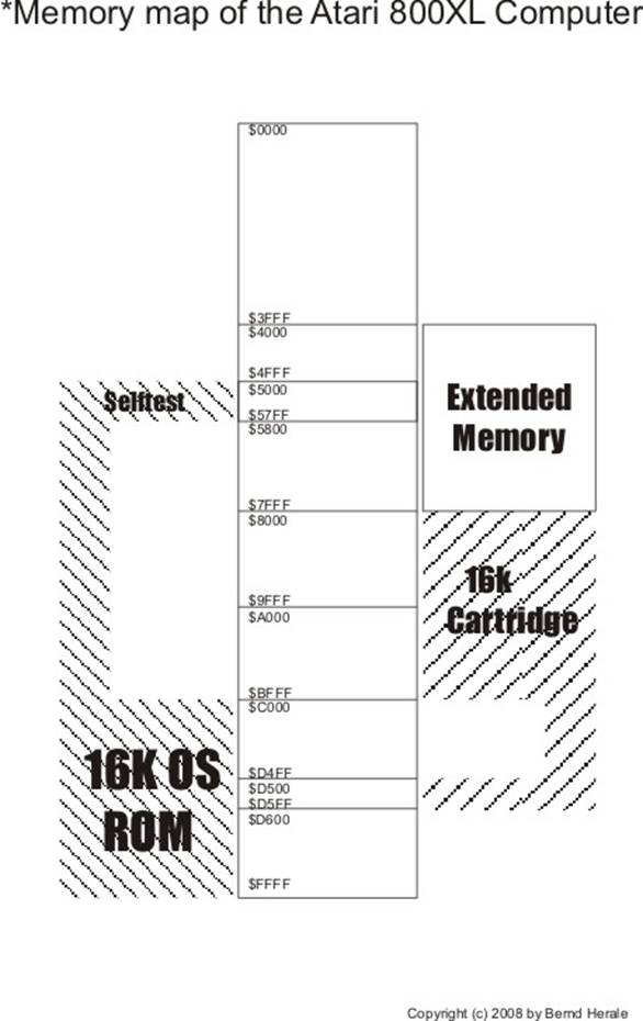
At the raw overview of the 800XL as memory arrangement some specialities of the Atari System become recognizable. The 16k OS (Operating system), nowadays known as „BIOS“, shares the upper memory with all system IC´s (not shown) and a little portion between $D500‐$D5FF with the cartridge port. The selftest is activated by setting PB7 to „0“ and is mirrored from $5000‐$57FF. The extended memory is at $4000‐$4FFF. Here´s the first problem of overlapping memory. PB7 shall be used for bank switching without activating the selftest. A logic in the GAL‐Chip suppresses the start of the selftest if additional memory is activated. Following outputs at the PB are used for the 512k mode of the memory extension:
MODE 512K RAMBO - 64 pages at 16k
| PB2=X | Choosen page of external memory – look at table |
| PB3=X | Choosen page of external memory – look at table |
| PB4=0 | 6502 CPU und Antic external memory access on |
| PB5=X | Choosen page of external memory – look at table |
| PB6=X | Choosen page of external memory – look at table |
| PB7=X | Choosen page of external memory – look at table |
| PB2 | PB3 | PB5 | PB6 | PB7 | Choosen page |
| 0 | 0 | 0 | 0 | 0 | 1 |
| 1 | 0 | 0 | 0 | 0 | 2 |
| 0 | 1 | 0 | 0 | 0 | 3 |
| 1 | 1 | 0 | 0 | 0 | 4 |
| * | * | * | * | * | **** |
| 1 | 1 | 1 | 1 | 1 | 64 |
PB4 switches on the additional memory for CPU and ANTIC. This method is also called „Rambo“.
MODE 256K RAMBO - 32 pages at 16k
| PB2=X | Choosen page of external memory |
| PB3=X | Choosen page of external memory |
| PB4=0 | 6502 CPU und Antic external memory access on |
| PB5=X | Choosen page of external memory |
| PB6=X | Choosen page of external memory |
| PB7 | Unused |
PB4 switches the CPU and PB5 the ANTIC to the additional memory. This method is also called „CompyShop“ ‐ method.
MODE 256K CompyShop 32 pages at 16k
| PB2=X | Choosen page of external memory |
| PB3=X | Choosen page of external memory |
| PB4=0 | 6502 CPU und Antic external memory access on |
| PB5=0 | Antic external memory access on |
| PB6=X | Choosen page of external memory |
| PB7 | Choosen page of external memory |

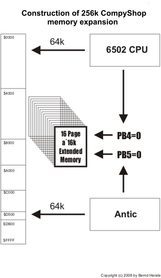
The two block diagrams show the different methods of accessing the additional memory.
Assembly of Hardware and Connections
The circuit just needs one GAL of the type 22V10 and one 512k Sram of the type BS62LV4005PC‐70. The prototype was connected directly to the CPU - which turned out to be an error. The CPU generated „Phi2“‐signal (the clock which all connected devices follow) got an extra charge from the GAL. That had bad affects to the signal. The square wave was more like a sawtooth wave with the result that memory access wasn´t always successful. Then it was connected to the ANTIC. There the „Phi2“‐signal got amplified by a TTL. To improve security the „Phi0“ was added to the linkage and provides together with the write‐signal a stable function even if the „Phi2“ is bad.

The violet signal shows the „Phi2“ output directly at the CPU, the yellow signal is „Phi2“ after amplification through the TTL in the Atari.
Wolfram (Mega‐Hz) successfully converted the circuit into a circuit board. Many thanks for that. Who as interested in it can get an extension from him. He´s currently the only provider.
At this point I´d also like to thank Hias and Mathy for their first class support creating the GAL code.
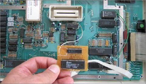
Prototype of 512k SRam expansion with a 16V8 Gal
1200XL inclusive 512k SRAM
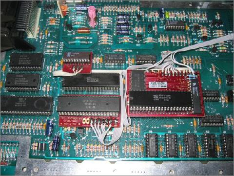
512k SRam built-in the 800XL expansion
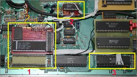
Picture 1: The ANTIC is to be removed from the 800XL´s circuit board and put into the new socket of the extension. The extensions circuit board connects into the ANTIC socket of the 800XL´s circuit board.
Picture 2: MMU connection board
Picture 3: PIA with line connectors from PB2 to PB4
The memory extension was tested with a 600/800/1200XL and 800/130XE. At the 130XE the additional 64k have to be deactivated to avoid faulty memory accesses from memory overlaps. The MMMU U3 is to be removed and replaced by bridges.
If it is an PAL or NTSC Atari can be determined by the C0xxxxx label at the ANTIC:
CO21698 PAL XL/XE - CO21697 NTSC XL/XE
The extension runs independet from the system and will work with both types.
For the ABBUC Hardware Contests HardwareDoc (Christoph Büssow) and me have put together an 800XL with all extensions. Thanks to Christoph´s Bios4Config no switches for the mode settings are necessary. The extension can be configured using the display of the Bios4Config. But the Bios4Config is not necessarily to run the 512k extension.
At the display XRAM is accessible via the menu key and will switch through the following states using UP and DOWN:
. XRAM=Off ------------------ Memory off.
· XRAM=256C ---------------- 256kbyte CompyShop on
· XRAM=256R ---------------- 256kbyte Rambo on
· XRAM=512k ---------------- 512kbyte Rambo on
All memory banks are in the range from Hex $4000 to $7FFF, decimal 16384 to 32767 and are switched with memory address Hex $D301, decimal 54017. To access the Rambo memory extension from Basic it has to be activated with Poke 54017,237 first. Then the banks can be called by using Poke 54017,xxx with the corresponding decimal number, for example „Poke 54017,71“ for Bank 9. The extension can be switched of using Poke 54017,253. In CompyShop mode the ANTIC access is turned on with Poke 54017,221, CPU with Poke 54017,237 and both together with Poke 54017,205. ATTENTION! Even Basic uses the memory range from $4000‐$7FFF if the program has a big size.
List of memory Banks in 512k Rambo mode
| Bank Nr. | HEX=$D301 | Dezimal=54017 |
| 0 | $EF | 237 |
| 1 | $EB | 233 |
| 2 | $E7 | 229 |
| 3 | $E3 | 225 |
| 4 | $CF | 207 |
| 5 | $CB | 203 |
| 6 | $C7 | 199 |
| 7 | $C3 | 195 |
| 8 | $AF | 175 |
| 9 | $AB | 171 |
| 10 | $A7 | 167 |
| 11 | $A3 | 163 |
| 12 | $8F | 143 |
| 13 | $8B | 139 |
| 14 | $87 | 135 |
| 15 | $83 | 131 |
| 16 | $6F | 111 |
| 17 | $6B | 107 |
| 18 | $67 | 103 |
| 19 | $63 | 99 |
| 20 | $4F | 79 |
| 21 | $4B | 75 |
| 22 | $47 | 71 |
| 23 | $43 | 67 |
| 24 | $2F | 47 |
| 25 | $2B | 43 |
| 26 | $27 | 39 |
| 27 | $23 | 35 |
| 28 | $F | 15 |
| 29 | $B | 11 |
| 30 | $7 | 7 |
| 31 | $3 | 3 |
List of memory Banks in 256k Rambo mode
| Bank Nr. | HEX=$D301 | Dezimal=54017 |
| 0 | $EF | 237 |
| 1 | $EB | 233 |
| 2 | $E7 | 229 |
| 3 | $E3 | 225 |
| 4 | $CF | 207 |
| 5 | $CB | 203 |
| 6 | $C7 | 199 |
| 7 | $C3 | 195 |
| 8 | $AF | 175 |
| 9 | $AB | 171 |
| 10 | $A7 | 167 |
| 11 | $A3 | 163 |
| 12 | $8F | 143 |
| 13 | $8B | 139 |
| 14 | $87 | 135 |
| 15 | $83 | 131 |
List of memory Banks in 256k CompyShop mode
| Bank Nr. | HEX=$D301 | Dezimal=54017 |
| 0 | $EF | 237 |
| 1 | $EB | 233 |
| 2 | $E7 | 229 |
| 3 | $E3 | 225 |
| 4 | $AF | 173 |
| 5 | $AB | 169 |
| 6 | $A7 | 165 |
| 7 | $A3 | 161 |
| 8 | $6F | 109 |
| 9 | $6B | 105 |
| 10 | $67 | 101 |
| 11 | $63 | 98 |
| 12 | $2F | 45 |
| 13 | $2B | 41 |
| 14 | $27 | 37 |
| 15 | $23 | 33 |
Addendum: schematic diagram including pin assignment and GAL listing.
Have fun clonig it,
Bernd Herale

